$2B Semiconductor Packaging, Testing Campus Gets Key Approval

Amkor Technology received approval from the Peoria City Council last night to build a more than 500,000-square-foot, $2 billion advanced semiconductor packaging and test facility—the largest outsourced advanced packaging plant in the U.S.—in a multi-phase project that will bring 2,000 jobs to the Arizona community.
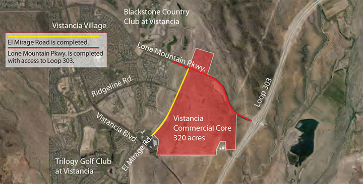
Called a pivotal milestone in advancing semiconductor manufacturing within the U.S., the 55-acre campus will be built at Five North at Vistancia, a 320-acre mixed-use lifestyle and employment core that is part of the larger Vistancia master-planned community located about 40 miles northwest of downtown Phoenix. The first phase of the state-of-the-art manufacturing plant is targeted to be ready within the next two to three years and the final buildout must be finished by Sept. 30, 2034.
The plant will package and test semiconductor chips that will be produced for Apple at the $40 billion Taiwan Semiconductor Manufacturing Co. facility located about 10 miles from the Vistancia site. Amkor, based in nearby Tempe, Ariz., said Apple will be its first and largest customer at the plant when it opens.
Amkor, the world’s largest U.S.-headquartered outsourced semiconductor assembly and test service provider, has been located in the Greater Phoenix area since 1984. The company’s plans for the new Peoria facility call for it to support critical markets including high-performance computing, automotive and communications. Giel Rutten, Amkor’s president & CEO, said in a prepared statement last night they were excited and proud to help spearhead the development of a robust American semiconductor ecosystem in the heart of the ‘Silicon Desert.’
READ ALSO: How Reshoring Is Driving Industrial Real Estate Demand
Mayor Jason Beck said in prepared remarks he was proud of the Peoria team that was bringing the project and high-quality jobs to Peoria, state of Arizona and U.S.
Amkor is seeking funding from the $280 billion federal CHIPS and Science Act. As part of the program, the federal government will award $39 billion to U.S. companies in competitive grants to finance construction, expansion or modernization of facilities and equipment for the semiconductor industry. On Monday, the U.S. Department of Commerce announced it would provide $1.5 billion direct funding from the CHIPS and Science Act to GlobalFoundries to expand its Malta, N.Y., semiconductor manufacturing facility, build a new 358,000-square-foot fab and modernize its Essex Junction, Vt., facility. GlobalFoundries produces essential chips for automotive, IoT, aerospace, defense and other vital markets.
Project details
The Peoria property is owned by Vistancia Development LLC, (VDV) which has agreed to sell the development site to Amkor. Under a three-way joint development agreement between VDV, Amkor and the city, VDV will build the roads and provide utility delivery to the development with the city reimbursing about $3 million toward the cost of the public infrastructure.
Amkor must close on the land acquisition by the end of October and begin construction on or before Sept. 30, 2025. Failure to do so will result in the loss of land and water rights.
The development agreement calls for Amkor to develop one or more facilities in Peoria with a minimum capital investment of $350 million in the first phase and an additional $350 million in the second phase.
Under Phase One, Amkor must employ at least 550 full-time employees no later than Sept. 30, 2029, with two other employment milestones set for September 2027 (300 employees) and September 2028 (425 employees). The company must also have completed the design, construction and begun operation of at least one manufacturing facility including all ancillary support systems and buildings by the end of phase one.
By phase two, Amkor will have to employ an additional 300 full-time employees for a total of 850 workers on the property. While the company will have to make an additional $350 million investment in capital expenditures, it does not need to expand the size or footprint of the facility.
The development agreement sets out penalties and fines, including paying $5,000 per month until the employment milestones are reached.
The post $2B Semiconductor Packaging, Testing Campus Gets Key Approval appeared first on Commercial Property Executive.


